Your current location: Home > APPLICATIONS

X-ray industrial CT technology can non-destructively and with high precision obtain internal images of integrated circuits, enabling the identification of defects within internal structures such as solder joints and pins. As a result, it finds widespread application in quality monitoring and failure analysis during the production of electronic products, contributing to enhanced product quality.
Industrial CT can clearly showcase the internal structures of a tested chip through two-dimensional slices and three-dimensional models, enhancing the ability to identify and locate internal defects.
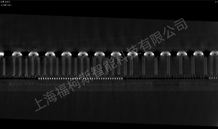
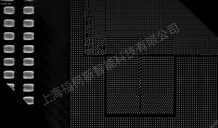
Industrial CT can inspect BGA (Ball Grid Array) soldering, non-invasively verifying the quality of solder joints.
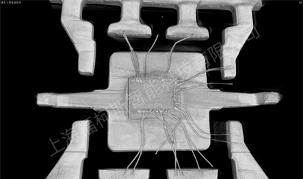
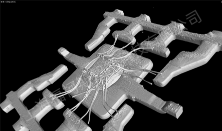
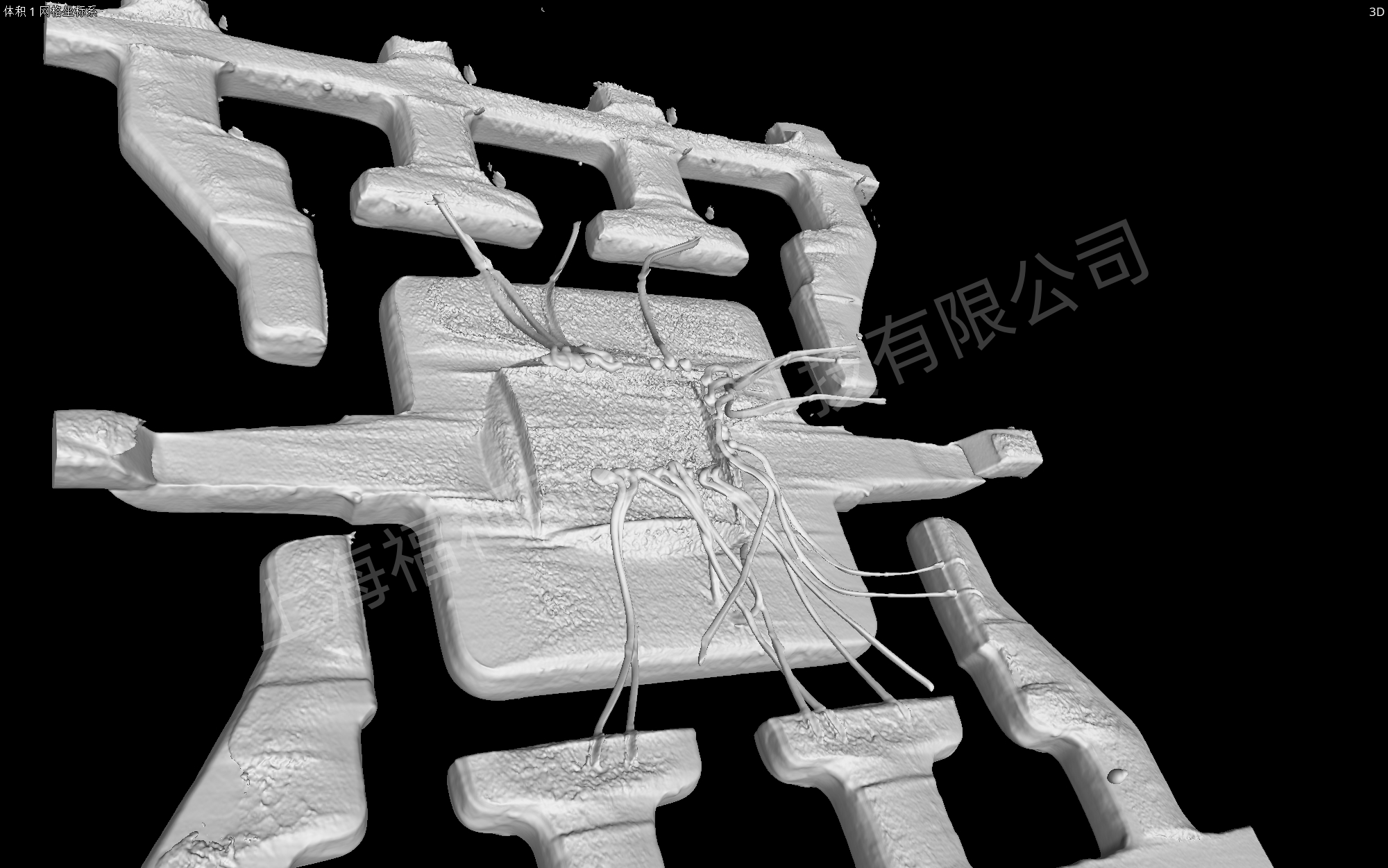
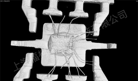
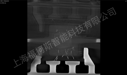
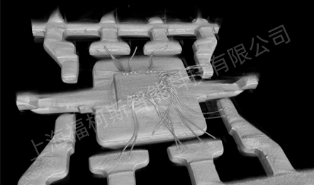
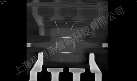
Through scanning encapsulated microcircuits, industrial CT can detect lead bonding and chip delamination, voids and cracks in molding compounds, the wireframe, and adhesive areas of the chip. This accurate defect localization increases the reliability of encapsulated microcircuits during their operational life.
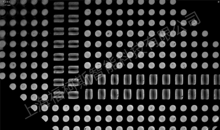
Industrial CT can also identify defects in ceramic capacitors, such as internal delamination, cracks, and voids.
Image display
Recommended Machine


- service@focus-sh.net
- (086) 021-31019175
- Room 102, Building 1, No.18, Handu Rd., Pudong New Area, Shanghai

Copyright © 2023 上海福柯斯智能科技有限公司 All Rights Reserved. 沪ICP备2023025604号-1

